NeoScope microscope delivers improved magnification
Jeol USA
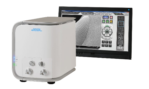
Jeol has unveiled the latest NeoScope Scanning Electron Microscope (SEM) with improved design.
The NeoScope is a high resolution SEM that produces images with a large depth of field at magnifications ranging from 10X - 60,000X.
Features include:
- Both high and low vacuum operation
- Three selectable accelerating voltages
- Secondary electron and backscattered electron imaging
- A touch screen interface
The NeoScope accommodates samples up to 70mm in diameter and 50mm in thickness. Both conductive and non-conductive samples can be examined. Optional EDS is available for elemental analysis.
More stories
Scanning Electron Microscopy applied to porous materials download
This document provides an appraisal of high resolution Scanning Electron Microscopy applied to porous materials.
Ultra-high resolution analytical field emission SEM
High performance FE-SEM optimised for sub-nm resolution imaging of any type of sample
Jeol launches EDS for rapid elemental mapping
Jeol has developed Centurio, an energy dispersive spectrometer (EDS) for ultra-fast and ultra-sensitive collection of X-rays through analysis with its scanning transmission electron microscopes.
Jeol TEM suited to high-throughput nano-analysis
The JEM-2800 from Jeol is a 200kV transmission electron microscope that delivers high-throughput nano-analysis for process and quality control of mass-produced semiconductor and materials samples.
Navigation system designed for SEM and EPMA users
Jeol is offering a 'point-and-shoot' navigation system that makes finding precise locations on a sample both fast and easy for SEM and EPMA users.


