WITec’s TrueSurface microscopy is now available as an integrated option for the alpha300 microscope range.
This development enables topographic Raman Imaging on large samples for the full range of WITec instruments.
The new imaging mode is also available as an upgrade for installed alpha300 and alpha500 systems.
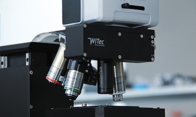
The functional core of the measurement mode is the sensor for optical profilometry, now fixed in the microscope objective turret.
The system measures the surface topography of large samples and correlates it with confocal Raman microscopy.
This allows very rough or heavily inclined samples to be chemically characterized precisely, automatically and easily while also being confocally imaged.
“Our customers have with every WITec system the possibility to undertake macroscopic investigations along the surface of a sample on the millimeter-scale, while performing microscopic 3D Raman Imaging measurements on the sub-micron scale” explained Dr. Olaf Hollricher, WITec co-founder and managing director R&D.
“The pioneering integration of an optical profilometer in a Raman microscope opens to scientists new possibilities in surface analysis”.


